Japanese semiconductor companies visit Dholera as part of a crucial step to support India’s ambitions of becoming a global hub for semiconductor manufacturing. A high-level delegation of 20 companies from Japan’s semiconductor ecosystem toured the Dholera Special Investment Region (SIR) this week, signaling strong interest in India’s rapidly growing chip-making industry.
The visit comes at a time when India is aggressively pursuing semiconductor self-reliance, with policies, incentives, and infrastructure development aimed at attracting leading global players. This development marks a turning point in India-Japan collaboration, bringing together Japanese precision and India’s scale to build a world-class semiconductor ecosystem.
Why the Visit Matters
The Japanese delegation included senior representatives from globally recognized companies, such as Shimizu Corporation, Japan, a firm known for excellence in infrastructure and precision engineering. Their visit follows SEMICON India 2025, where India highlighted robust fiscal incentives, policy stability, and an enabling ecosystem for chip-making industries.
This visit demonstrates Japan’s willingness to integrate its expertise in semiconductor equipment, specialty materials, and advanced components with India’s infrastructure and workforce readiness.
Key Meetings at Dholera SIR
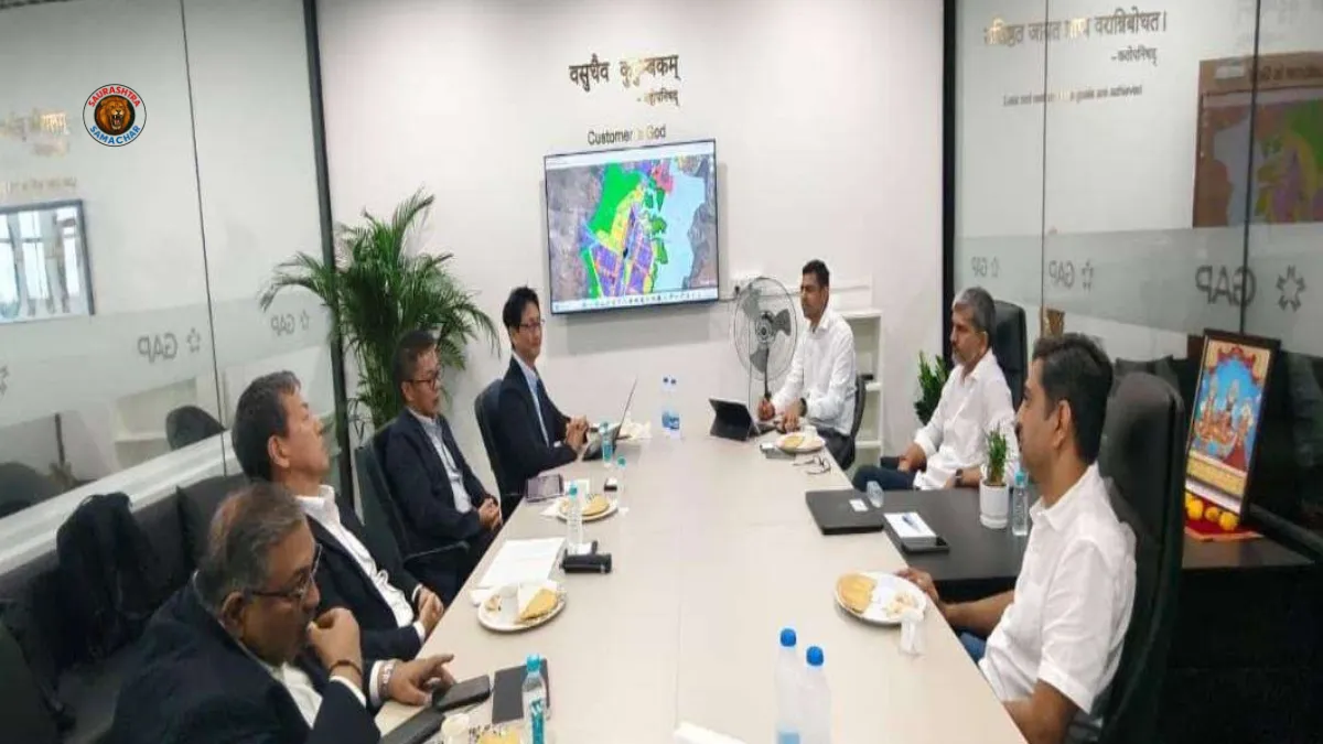
The Japanese delegation visited the ABCD Building, the central administrative hub of Dholera SIR. Representatives from Shimizu Corporation met with GAP Group, one of western India’s leading real estate and infrastructure developers, which has been the first mover in Dholera’s Activation Zone.
The discussions revolved around combining Japanese technological leadership with Dholera’s smart city infrastructure. The aim is to position Dholera not just as India’s semiconductor hub but as a globally competitive region for the electronics supply chain.
India’s Semiconductor Ambitions
India is already witnessing historic progress in semiconductor manufacturing. The ₹92,000 crore Tata Electronics semiconductor fabrication plant (fab), being developed in collaboration with Taiwan’s PSMC, is underway at Dholera.
The plant is expected to begin production by 2027, creating thousands of direct and indirect jobs. Alongside this, other projects like Renew Energy, INOX Air, Polycab, and a 5GW solar park are being developed in Dholera’s Activation Zone, likely to generate more than 1.5 lakh jobs.
GAP Group’s Role in Building Dholera
The GAP Group showcased its comprehensive development portfolio to the Japanese companies. Their offerings include:
- Industrial parks with ready-to-use factory spaces
- Residential projects such as Akhilam Township and Greenera Garden Villa
- Premium housing units under the Avant project with 1,000 homes
- Studio apartments like Aakar Premium for professionals
- GAP Industrial Park, offering 40,000 sq. m of ready industrial space
These projects aim to provide a seamless entry route for global semiconductor players by offering living, working, and industrial solutions in one integrated ecosystem.
Voices from the Leaders
Ambrish Parajiya, Managing Director of GAP Group, stated:
“The visit by Japanese semiconductor companies is a strong endorsement of India’s vision and Dholera’s infrastructure readiness. Japan’s unmatched precision and reliability complement India’s scale and market potential. At GAP Group, we are committed to supporting this strategic partnership by providing world-class infrastructure, ensuring Dholera becomes India’s Semiconductor City.”
Opportunities for Japanese Companies
The delegation explored diverse opportunities for collaboration, such as:
- Setting up precision facilities for Japanese SMEs to supply components to the Tata Semiconductor Fab
- Establishing warehousing and gas distribution systems
- Building clean rooms and advanced engineering units
- Partnering in skill development programs to train Indian engineers and technicians
- Providing accommodation for Japanese managers, expats, and engineers through premium residential projects
This reflects a strong intent to not just supply to India but also to integrate with the local workforce and community.
Dholera’s Strategic Advantage
Dholera is one of India’s most strategically planned regions:
- Location: 110 km from Ahmedabad along the Delhi–Mumbai Industrial Corridor
- Area: 927 sq. km, designed as India’s first Platinum Greenfield Smart City
- Connectivity: Upcoming Ahmedabad–Dholera Expressway and an international airport set to begin operations by December 2025
- Green Infrastructure: Focus on renewable energy, sustainable urban planning, and cutting-edge logistics facilities
Such infrastructure makes Dholera an ideal destination for large-scale, long-term investments in semiconductor manufacturing.
GAP Group’s Track Record
GAP Group is credited with being a pioneer in the Activation Zone:
- Delivered the first RERA-approved villa project
- Developed the first industrial park in the region
- Launched the first premium 1BHK housing project
- Committed to ₹2,500 crore investment in real estate over the next five years
- Recently secured No Objection Certificate (NOC) from the Airports Authority of India for its Avant project
This strong foundation has helped Dholera gain credibility among international investors, including Japanese semiconductor companies.
Japanese Semiconductor Companies Visit Dholera: A Win-Win Collaboration
The collaboration between India and Japan in semiconductors is not only about manufacturing chips but about creating a resilient supply chain. Japan’s leadership in equipment, raw materials, and precision engineering blends perfectly with India’s talent pool, market size, and infrastructure ambitions.
This partnership has the potential to reduce global semiconductor supply chain risks while also making India a new powerhouse in electronics and advanced technology.
Informative Table: Key Highlights of the Visit
| Key Aspect | Details |
|---|---|
| Delegation | 20 Japanese semiconductor companies |
| Key Firms | Shimizu Corporation and others |
| Location | Dholera Special Investment Region (SIR), Gujarat |
| Meetings | GAP Group & Dholera officials |
| Focus Areas | Semiconductor fabs, industrial parks, skill training, infrastructure |
| Major Indian Project | Tata–PSMC Semiconductor Fab (₹92,000 crore) |
| Jobs Expected | 1.5 lakh+ (direct & indirect) |
| Connectivity Boost | Ahmedabad–Dholera Expressway, International Airport (2025) |
The Road Ahead
With the Tata Fab expected to start operations in 2027, Dholera will soon emerge as India’s Semiconductor City. The involvement of Japanese semiconductor companies strengthens this vision and ensures India gains access to top-tier global expertise.
The Indian government’s continuous policy push, coupled with private sector investments and Japan’s trust, positions Dholera as a model semiconductor hub for the future.
Also read: Dholera Smart City and Gujarat’s Mega Vision for Vibrant Regional Growth
Conclusion
The recent development where Japanese semiconductor companies visit Dholera represents more than just a business trip. It reflects growing global confidence in India’s semiconductor ambitions, Dholera’s readiness, and the India–Japan partnership.
As the world grapples with semiconductor shortages and the need for resilient supply chains, India’s proactive moves in Dholera could prove transformative. If executed well, this collaboration has the power to reshape the global semiconductor map, making Dholera not just a city but a symbol of India’s technological rise.